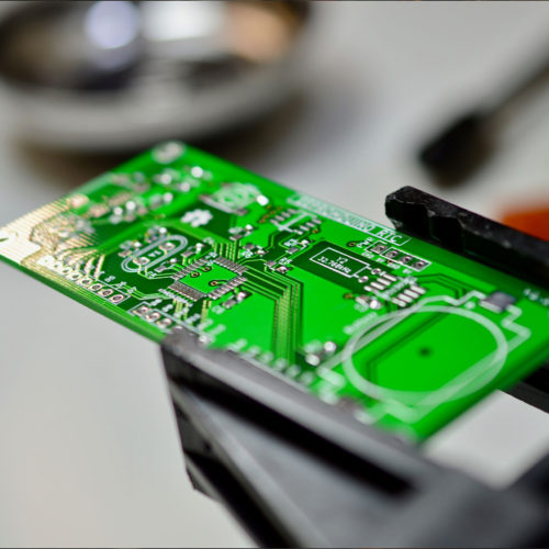
PCB & PCBa

Design for PCBs, surface finishing and component sourcing

One Point Zero focus on the finer detail of our client’s projects to create innovative PCB layouts for successful projects.

We have a proven track record in sourcing highly reliable components with competitive prices. We cover the early stages of principle design all the way to mass production.

Our engineers know that good PCB layout is critical to the electronics design properly working. We work to get it right the first time, each time.

PCB-design

Key areas

Board outline

PCB designs come in various shapes, created to fit in to the enclosures, make assembly easier or reduce the overall impression of size.
There are cost implications to making unusual-shaped boards as they can increase material wastage.. These cost implications need to be balanced against ease of manufacture, service, repair, form factor and use.

PCB materials

Beyond deciding whether the PCB should be rigid, flexible or a combination, the material selection and layer stack is important.
Many PCBs are made from woven fiberglass cloth and epoxy resin. There are a wide range of grades and thicknesses depending upon the application which our team carefully chose depending on the product requirements and usecase.

Component Sourcing

There is always a wide selection of electrical compments to chose from, but not all of them will do the job effectvely or reliably.
More often than not, you pay for what you get and the cheap option will fail quickly and wont stand up to the high standards consumers expect.
Our team have experience in establishing the base electrical requirements for a product and sourcing the most stable and cost effective solutions to hit spec and maintain reliablility.

Track geometry

When schematics are drawn it’s important to route the track design efficiently and effectively to minimise material wastage. It’s useful to indicate which connections have special attributes and to set design rules up for these which could include simple attributes for high current traces that need to be a minimum width or depth.
Our team apply these attributes to the PCB which are used when creating tracking, copper planes and for verification checking at the end of the design.

Thermal management

Electronics produce heat. Copper areas in the PCB can help to distribute the heat over a wider area and act as a heatsink.
Many components incorporate a thermal pad, often connected to ground, which is used to thermally conduct heat from the device.
One Point Zero engineers take care to ensure that this heat distribution, and the placement of other heat generating components doesn’t cause others to heat up beyond their specification causing incorrect operation or failure.

Silk Screening

PCBs can have up to two silkscreen layers. These are non-conductive text, markings, warnings and identification labels that can assist during assembly, test and installation.
Common uses of silkscreen are to indicate the polarity of components such as diodes and capacitors, indicate the pin 1 reference on ICs, identify test points, show the PCB part and revision number, provide warning symbols for high-voltage, ESD care, and to label each terminal on a connector that is manually wired to the board.